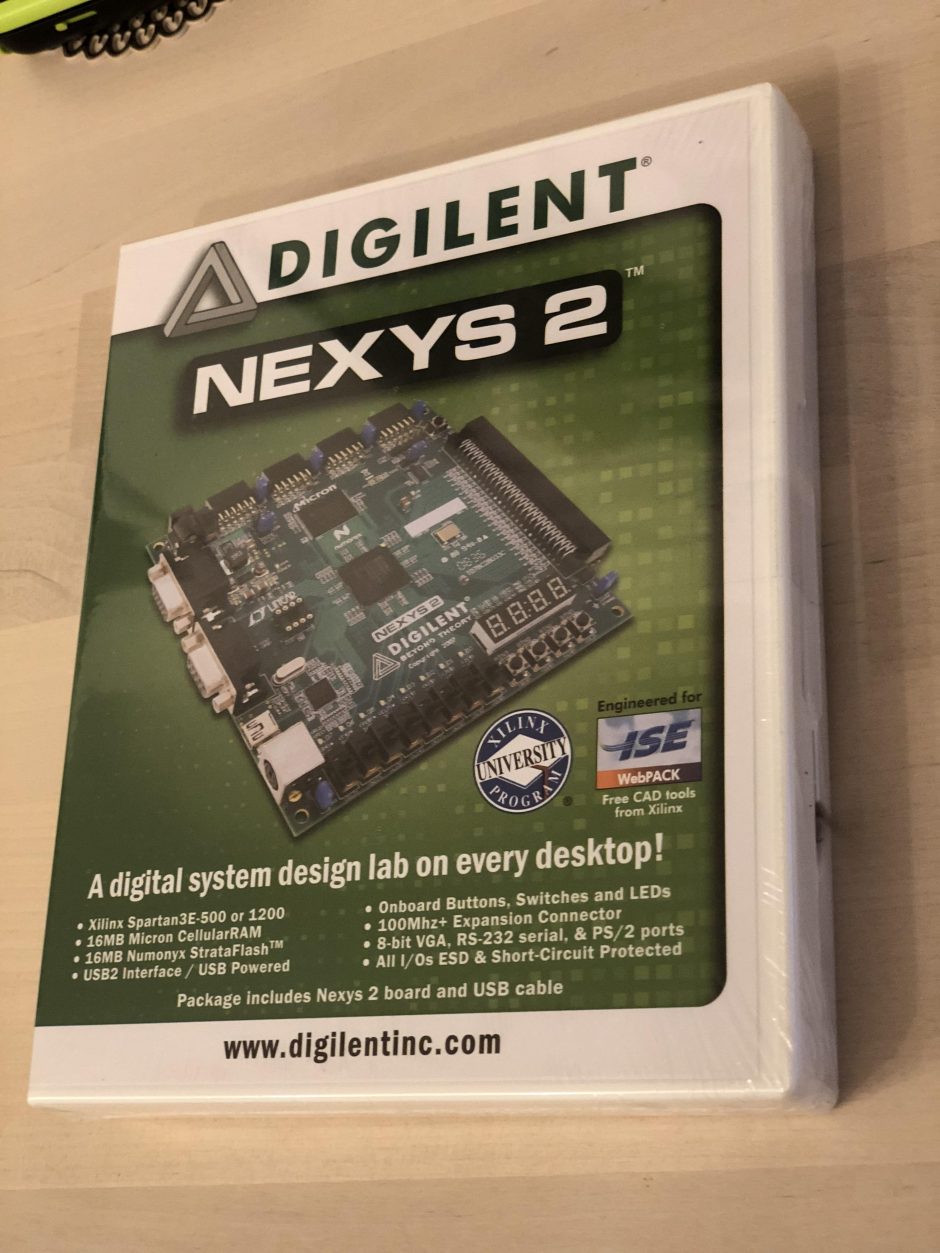
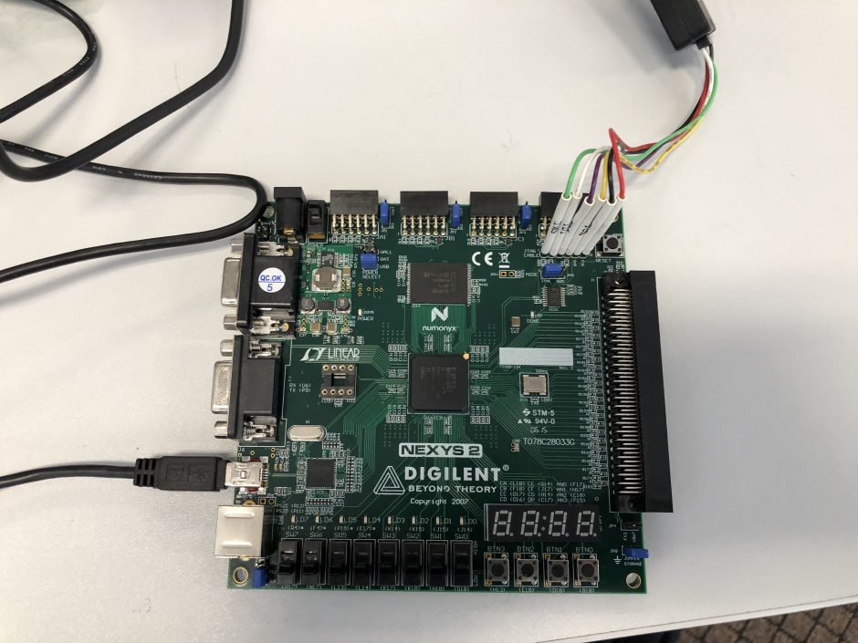
Ordered a vintage FPGA from 2007, Nexys2 – 1200, the description / seller looked very good and the condition was used, so I ordered it, what issue can happen with a tested and “new” condition FPGA? 🙂
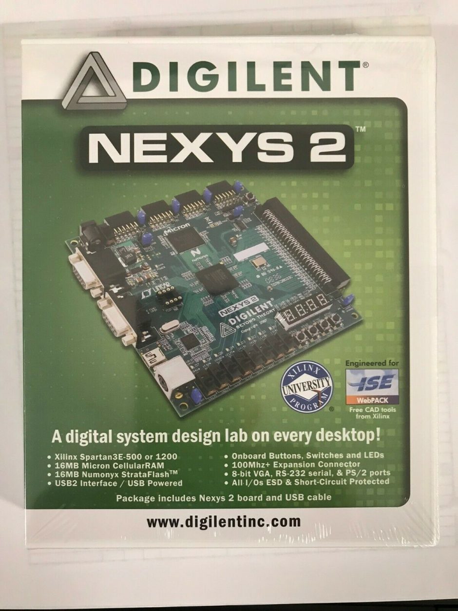
When the box appeared it, was in foil.
It was a bit weird, how can be in factory foil a 2007 (this time 12 year old FPGA), but nevermind, it was more interesting, that I will be the first user of the unit.
So let’s see it closer, I was very happy.
Original box was cracked, even it was foiled.
This time I had not worry about.
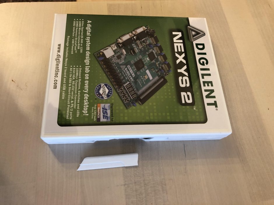
After removing the foil, the issue was bigger, but never mind, it is a safety holder
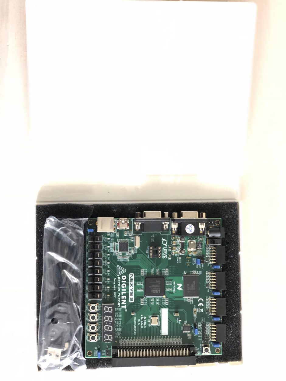
The FPGA looked unaffected by the damage, there was no any crack or issue on the FPGA side
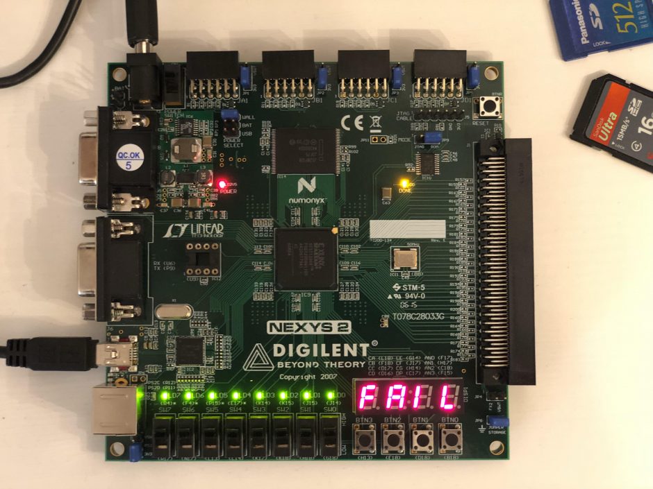
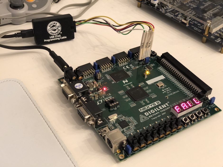
When I turned on the unit, the Factory installed self test gave a FAIL message, with error code 1.
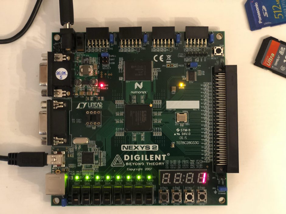
I did not see any crack or damage on the unit
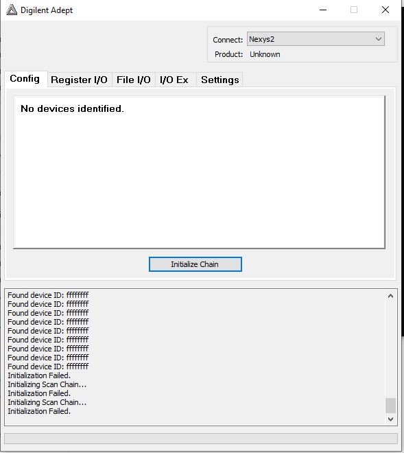
The first warning sign was that the Digilent Adept2 Software was not able to connect to the FPGA
The Unit was Re-funded, as a very good seller.
But this stage I did not give up, I really want to undersstand what causing such weird issue for FPGA-s.
I checked the user manual, which stating few possible root causes:
https://reference.digilentinc.com/reference/programmable-logic/nexys-2/reference-manual
Built in Self TestA demonstration configuration is loaded into the Platform Flash ROM on the Nexys2 board during manufacturing. This demo, also available on the resource CD and on the Digilent website, can serve as a board verification test since it interacts with all devices and ports on the board. To configure the FPGA from a bit file stored in Platform Flash, set the Mode Jumper to Slave Serial and cycle power or press the FPGA reset button.The self-test checks the on-board memories, and then connects the switches to the LEDs, the buttons and PS/2 keyboard (if attached) to the seven-segment display, and a VGA monitor (if attached) will show a color pattern. If the on-board memories pass test, “PASS” will be displayed on the seven-segment display (otherwise, “FAIL”). After the memory test, the buttons and switches will drive the LEDs and seven-segment display, so that all user I/O devices can be manually checked.If the self test is not resident in the Platform Flash ROM, it can be programmed into the FPGA or reloaded into the ROM using the Adept programming software.All Nexys2 boards are 100% tested during the manufacturing process. If any device on the Nexys2 board fails test or is not responding properly, it is likely that damage occurred during transport or during use. Typical damage includes stressed solder joints, or contaminants in switches and buttons resulting in intermittent failures. Stressed solder joints can be repaired by reheating and reflowing solder, and contaminants can be cleaned with off-the-shelf electronics cleaning products. If a board fails test within the warranty period, it will be replaced at no cost. If a board fails test outside of the warranty period and cannot be easily repaired, Digilent can repair the board for a fee. Contact Digilent for more details.
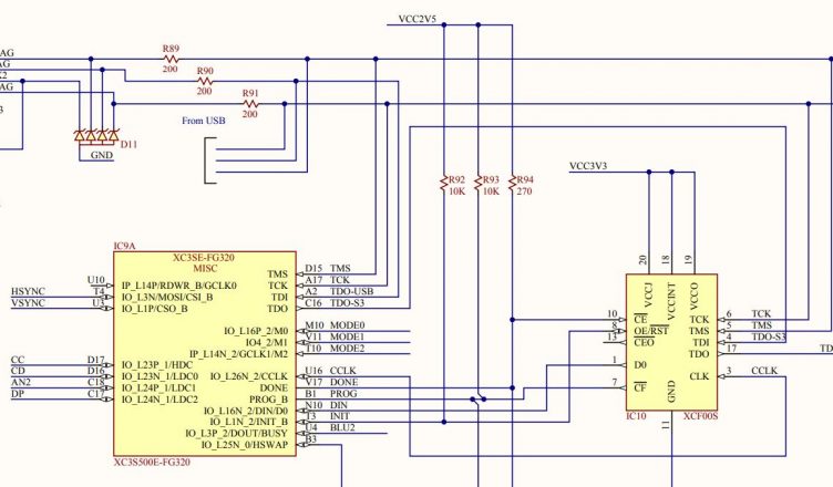
As stated in the manual, simply a transport problem can cause the problem with causing some soldering cracks. Before touching this, I checked and started to analyze what FAIL 1 error code means. It is simply a Memory problem.
Quting the Description of the Nexys2 Memory Test Software
——————————
——————————
————
— Behavioral description
——————————
——————————
————
— PhoenixOnBoardMemTest implements the following registers:
——————————
——————————
————
— The component implements a set of 7 Epp registers (read only)
— for PC interface (via USB):
— Register Function
— ——– ——–
— 0 Test Status register
— 1 Memory address bits 0-7
— 2 Memory address bits 8-15
— 3 Memory address bits 16-23
— 4 Expected Data bits 0 – 7
— 5 Expected Data bits 8 – 15
— 6 Read Data bits 0 – 7
— 7 Read Data bits 8 – 15
—
— The registers can be read at any time, but registers 1 – 7 only
— provide steady values after the test ends(see test description below)
— Test description:
— There are three sub-tests implemented:
— The RAM test:
— Write RAM (status = 0x00)
— Writes the whole RAM on the Nexys board with a sequence of
— 16 bit words, as below:
— 0x0000, 0x0001, 0x0002, … 0xfffe, 0x0000, …
— Skiping value 0xffff, avoids address – data matching for all
— the memory range.
— Read RAM (status = 0x02)
— Reads back the whole RAM and compares to the data pattern above.
— If no differencies, continues with the Flash QRY test.
— If a difference, the test ends with an RAM error message:
— RAM error message (status alternates 0x03, 0x01)
— Test is ended and the 7-seg displays alternate the messages:
— FAIL, 1
— In this state:
— – registers 1, 2, 3 show the ADR+2 (ADR = mismach address)
— – registers 4, 5 show the ExpData+1 (ExpData = expected data)
— – registers 6, 7 show the actual RAM data.
— Flash QRY test:
— Set Flash chip in “read QRY” mode (status = 0x06)
— Read Flash QRY (status = 0x04)
— Read Flash addresses 0x000020, 0x0000022, 0x000024 and compare
— to the string “0x0051, 0x0052, 0x0059” (ASCII codes for “QRY)
— If no differencies, continues with the Flash IDC test.
— If a difference, the test ends with an QRY error message:
—
— QRY error message (status alternates 0x05, 0x07)
— Test is ended and the 7-seg displays alternate the messages:
— FAIL, 2
— In this state:
— – registers 1, 2, 3 show the ADR+2 (ADR = mismach address)
— – registers 4, 5 show the ExpData (ExpData = expected data)
— – registers 6, 7 show the actual RAM data.
— Flash IDC test:
— Set Flash chip in “read IDC” mode (status = 0x0c)
— Read Flash IDC (status = 0x0e)
— Read Flash addresses 0x000000, 0x0000001 and compare
— to the string “0x0089, 0x00yy, (Intel ID and Flash size codes:
— yy = 16 – 32Mbits
— yy = 17 – 64Mbits
— yy = 18 – 128Mbits
— yy = 1d – 256Mbits)
— If no differencies, continues with the set Flash in Array mode.
— If a difference, the test ends with an IDC error message:
—
— IDC error message (status alternates 0x0f, 0x0d)
— Test is ended and the 7-seg displays alternate the messages:
— FAIL, 3
— In this state:
— – registers 1, 2, 3 show the ADR+2 (ADR = mismach address)
— – registers 4, 5 show the ExpData (ExpData = expected data)
— – registers 6, 7 show the actual RAM data.
— Set Flash chip in “read array” mode (status = 0x0a)
— PASS message (status alternates 0x0b, 0x09)
— Test is ended and the 7-seg displays alternate the messages:
— PASS, zzzz (zzzz show the Flash sizs (in Mbits))
— In this state:
— – registers 1, 2, 3 show the 0x000006
— – registers 4, 5 show the ExpData (0x00ff)
— – registers 6, 7 show the actual RAM data (0x00yy).
— Test is running while the status is any even value (bit 0x01 = 0):
— 0x00, 0x02, 0x04, 0x06, 0x08, 0x0a, 0x0c, 0x0e
— Test is done while the status is any odd value (bit 0x01 = 1):
— 0x01, 0x03, 0x05, 0x07, 0x09, 0x0b, 0x0d, 0x0f
This would mean we have issue with the Memory Unit or the connection between the Memory or the FPGA chip
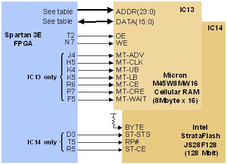
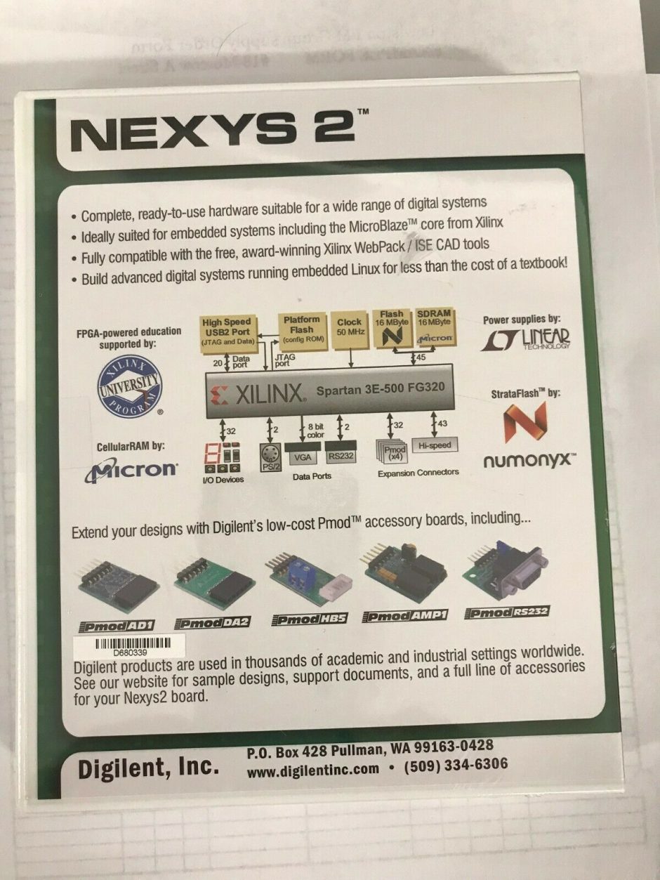
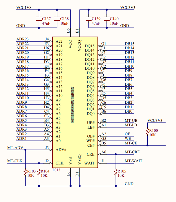
28Mbit Micron M45W8MW16 Cellular RAM pseudo-static DRAM device organized as 8Mbytes x 16bits. It can operate as a typical asynchronous SRAM with read and write cycle times of 70ns, or as a synchronous memory with an 80MHz bus. When operated as an asynchronous SRAM, the Cellular RAM automatically refreshes its internal DRAM arrays, allowing for a simplified memory controller design (similar to any SRAM) in the FPGA. When operated in synchronous mode, continuous transfers of up to 80MHz are possible.
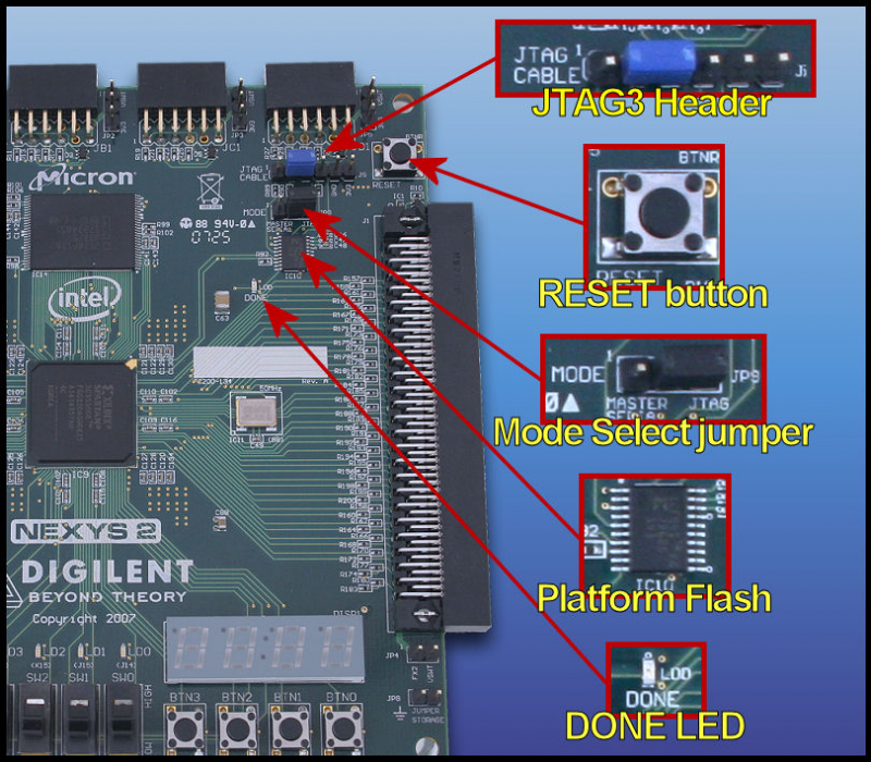
Before jumping to a fast track Re-Soldering or Memory replacement project, I was looking for a JTAG-USB or HS1 / HS2 / HS3 cable
Finally I could borrow one to see more closr this usse, as Mini USB connector was not working for the FPGA, but I was hoping at least JTAG headers will work
Under Xilinx Impact Utility, the JTAG connection started working immediately
Try doing some advanced thing, for example Erase the Platform Flash or Query the DeviceID, it always failed:
INFO:iMPACT – Digilent Plugin: no JTAG device was found.
AutoDetecting cable. Please wait.
*** WARNING ***: When port is set to auto detect mode, cable speed is set to default 6 MHz regardless of explicit arguments supplied for setting the baud rates
PROGRESS_START – Starting Operation.
Connecting to cable (Usb Port – USB21).
Checking cable driver.
Driver file xusb_emb.sys found.
Driver version: src=1029, dest=1029.
Driver windrvr6.sys version = 10.2.1.0. WinDriver v10.21 Jungo (c) 1997 – 2010 Build Date: Aug 31 2010 x86_64 64bit SYS 14:14:44, version = 1021.
Cable PID = 0008.
Max current requested during enumeration is 74 mA.
Type = 0x0004.
Cable Type = 3, Revision = 0.
Setting cable speed to 6 MHz.
Cable connection established.
Firmware version = 1303.
File version of C:/Xilinx/14.7/ISE_DS/ISE/
data/xusb_xlp.hex = 1303.
Firmware hex file version = 1303.
PLD file version = 0012h.
PLD version = 0012h.
PROGRESS_END – End Operation.
Elapsed time = 0 sec.
Type = 0x0004.
ESN device is not available for this cable.
Attempting to identify devices in the boundary-scan chain configuration…
INFO:iMPACT – Current time: 8/31/2019 8:38:59 AM
// *** BATCH CMD : Identify -inferir
PROGRESS_START – Starting Operation.
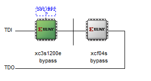
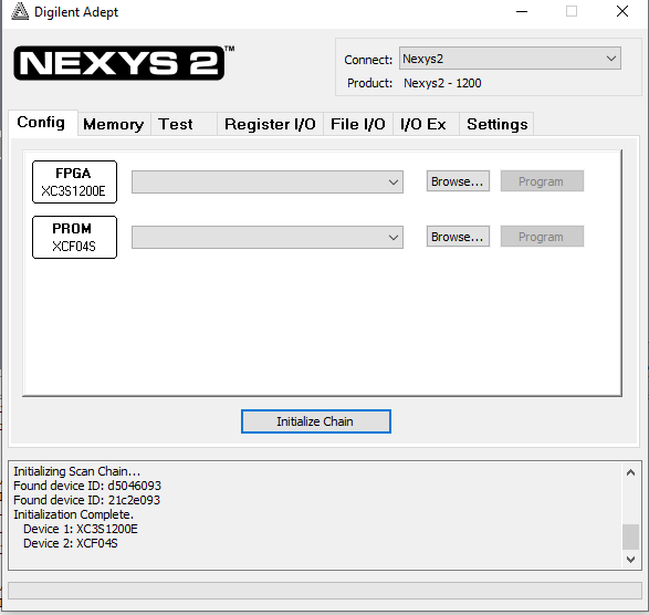
Identifying chain contents…’0′: : Manufacturer’s ID = Xilinx xcf04s, Version : 13
INFO:iMPACT:1777 –
Reading C:/Xilinx/14.7/ISE_DS/ISE/xcf/
data/xcf04s.bsd…
INFO:iMPACT:501 – ‘1’: Added Device xcf04s successfully.
——————————
——————————
———-
——————————
——————————
———-
‘1’: : Manufacturer’s ID = Xilinx xc3s1200e, Version : 2
INFO:iMPACT:1777 –
Reading C:/Xilinx/14.7/ISE_DS/ISE/
spartan3e/data/xc3s1200e.bsd..
.
INFO:iMPACT:501 – ‘1’: Added Device xc3s1200e successfully.
——————————
——————————
———-
——————————
——————————
———-
done.
PROGRESS_END – End Operation.
Elapsed time = 1 sec.
// *** BATCH CMD : identifyMPM
INFO:iMPACT – Current time: 8/31/2019 8:39:05 AM
// *** BATCH CMD : ReadIdcode -p 1
INFO:iMPACT:583 – ‘1’: The idcode read from the device does not match the idcode in the bsdl File.
INFO:iMPACT:1578 – ‘1’: Device IDCODE :
000011111111111111111111111111
10
INFO:iMPACT:1579 – ‘1’: Expected IDCODE:
00000001110000101110000010010011
You can see from the example above that this Spartan3’s Device IDCode does not match that should be for a Nexys2 Spartan3E 1200
Expected:
00000001110000101110000010010011
This device is:
000011111111111111111111111111
Let’s do some trick and more hacking, so I altered the Xilinx Boundary File like this DeviceID
NFO:iMPACT – Current time: 8/31/2019 8:31:11 AM
// *** BATCH CMD : Identify -inferir
PROGRESS_START – Starting Operation.
Identifying chain contents…’0′: : Manufacturer’s ID = Xilinx xcf04s, Version : 13
INFO:iMPACT:1777 –
Reading C:/Xilinx/14.7/ISE_DS/ISE/xcf/data/xcf04s.bsd…
INFO:iMPACT:501 – ‘1’: Added Device xcf04s successfully.
———————————————————————-
———————————————————————-
‘1’: : Manufacturer’s ID = Xilinx xc3s1200e, Version : 2
INFO:iMPACT:1777 –
Reading C:/Xilinx/14.7/ISE_DS/ISE/spartan3e/data/xc3s1200e.bsd…
INFO:iMPACT:501 – ‘1’: Added Device xc3s1200e successfully.
———————————————————————-
———————————————————————-
done.
PROGRESS_END – End Operation.
Elapsed time = 0 sec.
// *** BATCH CMD : identifyMPM
INFO:iMPACT – Current time: 8/31/2019 8:31:16 AM
// *** BATCH CMD : ReadIdcode -p 1
Maximum TCK operating frequency for this device chain: 10000000.
Validating chain…
INFO:iMPACT:1206 – Instruction Capture = ‘1111111111111101000100000001’
INFO:iMPACT:1207 – Expected Capture = ‘10101010101010XXXX01XXXXX001’
INFO:iMPACT:2130 – Boundary-scan chain test failed . Please check tdi->tdo connection between the cable and device:’1′ ( ‘xc3s1200e’).
A problem may exist in the hardware configuration.
Check that the cable, scan chain, and power connections are intact,
that the specified scan chain configuration matches the actual hardware, and
that the power supply is adequate and delivering the correct voltage.
This error means, it accepted the hacked DeviceID and entered into the next step, but the Instruction Capture stage failed with different bits recognized than expected.
The last step what we can do is to simply push the corrupt FPGA chip to get the soldering joints working manually
And suddenly everything started working, just until the FPGA chip was under push
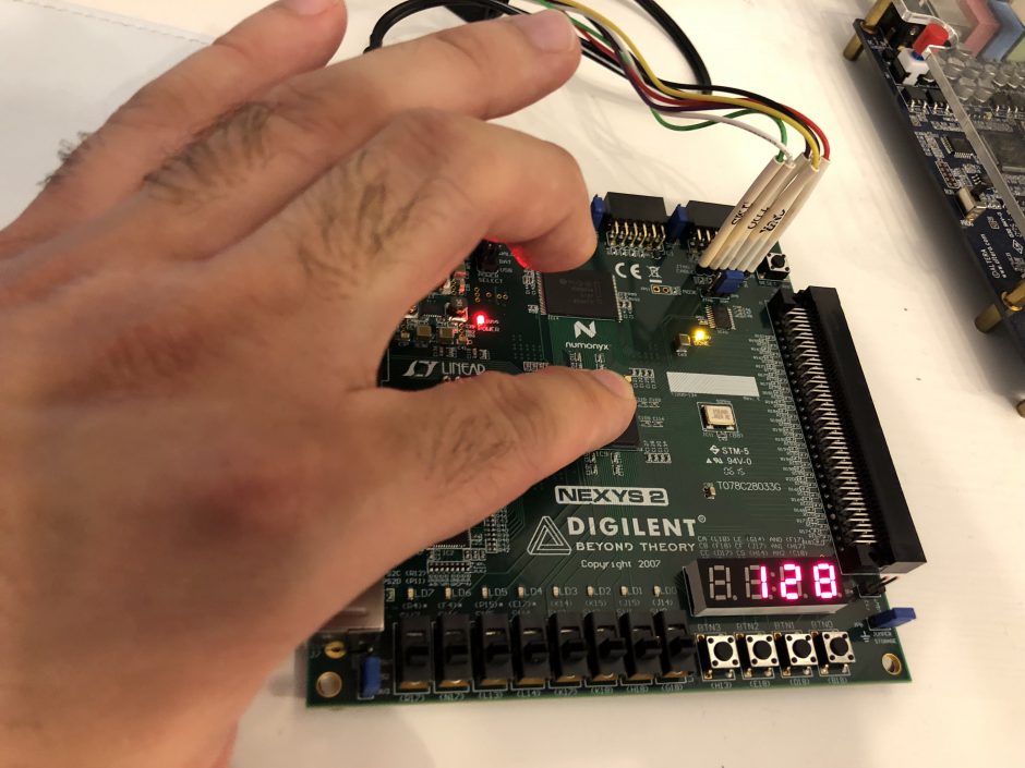
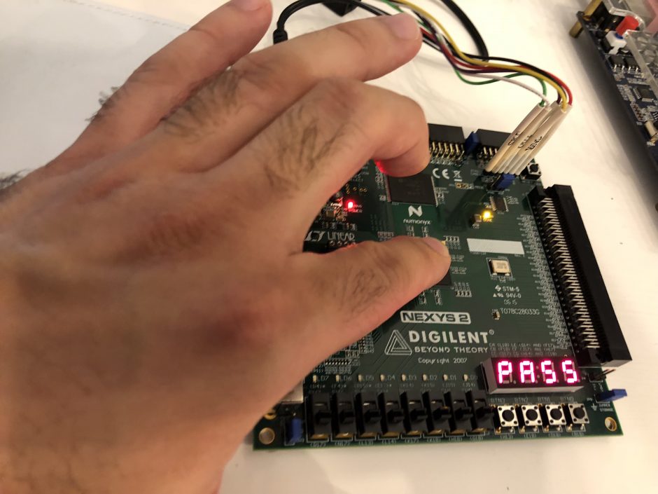
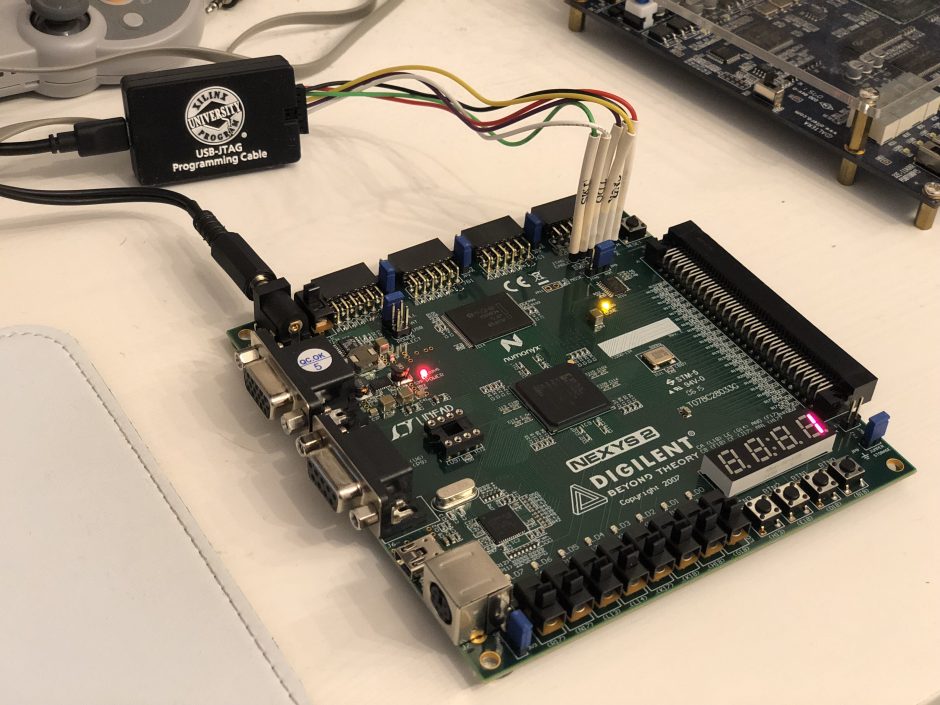
Internal Self test PASS, output code 128
Validated with both Digilent Adept2 Software on Mini USB
Validated additionally with JTAG-USB cable through Impact Software
// *** BATCH CMD : setCable -port auto
INFO:iMPACT – Digilent Plugin: Plugin Version: 2.4.4
INFO:iMPACT – Digilent Plugin: no JTAG device was found.
AutoDetecting cable. Please wait.
*** WARNING ***: When port is set to auto detect mode, cable speed is set to default 6 MHz regardless of explicit arguments supplied for setting the baud rates
PROGRESS_START – Starting Operation.
Connecting to cable (Usb Port – USB21).
Checking cable driver.
Driver file xusb_emb.sys found.
Driver version: src=1029, dest=1029.
Driver windrvr6.sys version = 10.2.1.0. WinDriver v10.21 Jungo (c) 1997 – 2010 Build Date: Aug 31 2010 x86_64 64bit SYS 14:14:44, version = 1021.
Cable PID = 0008.
Max current requested during enumeration is 74 mA.
Type = 0x0004.
Cable Type = 3, Revision = 0.
Setting cable speed to 6 MHz.
Cable connection established.
Firmware version = 1029.
File version of C:/Xilinx/14.7/ISE_DS/ISE/data/xusb_xlp.hex = 1303.
Firmware hex file version = 1303.
Downloading C:/Xilinx/14.7/ISE_DS/ISE/data/xusb_xlp.hex.
Downloaded firmware version = 1303.
PLD file version = 0012h.
PLD version = 0012h.
PROGRESS_END – End Operation.
Elapsed time = 0 sec.
Type = 0x0004.
ESN device is not available for this cable.
Attempting to identify devices in the boundary-scan chain configuration…
INFO:iMPACT – Current time: 8/31/2019 10:40:50 AM
// *** BATCH CMD : Identify -inferir
PROGRESS_START – Starting Operation.
Identifying chain contents…’0′: : Manufacturer’s ID = Xilinx xcf04s, Version : 13
INFO:iMPACT:1777 –
Reading C:/Xilinx/14.7/ISE_DS/ISE/xcf/data/xcf04s.bsd…
INFO:iMPACT:501 – ‘1’: Added Device xcf04s successfully.
———————————————————————-
———————————————————————-
‘1’: : Manufacturer’s ID = Xilinx xc3s1200e, Version : 2
INFO:iMPACT:1777 –
Reading C:/Xilinx/14.7/ISE_DS/ISE/spartan3e/data/xc3s1200e.bsd…
INFO:iMPACT:501 – ‘1’: Added Device xc3s1200e successfully.
———————————————————————-
———————————————————————-
done.
PROGRESS_END – End Operation.
Elapsed time = 0 sec.
// *** BATCH CMD : identifyMPM
INFO:iMPACT – Current time: 8/31/2019 10:41:00 AM
// *** BATCH CMD : ReadIdcode -p 1
Maximum TCK operating frequency for this device chain: 10000000.
Validating chain…
Boundary-scan chain validated successfully.
‘1’: IDCODE is ‘00100001110000101110000010010011’
‘1’: IDCODE is ’21c2e093′ (in hex).
‘1’: : Manufacturer’s ID = Xilinx xc3s1200e, Version : 2
When the push force removed and power cycled again, the issue came back again
Next step: re-solder / re-balling the FPGA chip 🙂
Share with: